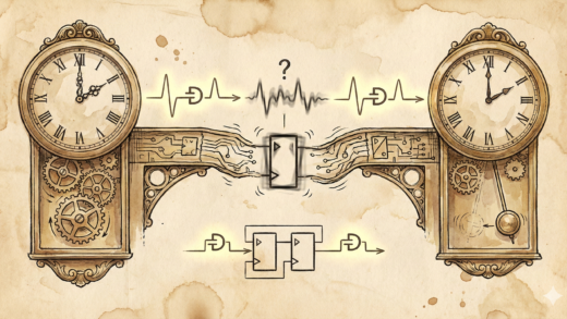

If you’ve spent more than a week in FPGA design, you know the feeling. You hit “Generate Bitstream,” go grab a coffee, and come back to see the dreaded red text: Timing Constraints Not Met.
But ignoring these errors or blindly applying “Synthesis Strategies” isn’t a solution. In high-reliability fields like avionics or automotive, a timing violation isn’t just a warning—it’s a potential metastability event waiting to happen in the field.
The XDC (Xilinx Design Constraints) or SDC (Synopsys Design Constraints) file is the contract you sign with the Static Timing Analysis (STA) engine. Today, we’ll move beyond the basics and dive into the technical mechanics of the four most critical command sets.
1. create_clock: Defining the Time Reference
The STA engine is purely mathematical. Without a reference period, it cannot calculate Setup (`Data Arrival < Data Required`) or Hold (`Data Arrival > Data Required`) slack.
However, defining a clock isn’t just about the frequency. A designer must also consider Jitter and Duty Cycle distortion. Furthermore, if you are interfacing with external synchronous devices (ADCs, SDRAMs), you must define Virtual Clocks.
The I/O delay constraints need a reference clock. If the external device’s clock doesn’t physically enter the FPGA (e.g., it shares a board-level oscillator), you cannot use `get_ports`. You need a virtual container to represent that external time domain.
2. set_input_delay & set_output_delay: System Level Budgeting
These are the most misunderstood commands in the history of FPGA design. Let’s be technically precise: These commands do NOT add delay lines inside the FPGA.
Instead, they subtract time from the global period budget. You are describing the physics of the PCB trace and the external IC’s datasheet parameters to the Vivado/Quartus analyzer.
A. Input Delay: The Data Arrival Equation
When an external chip sends data to the FPGA, the data is valid only after a certain delay relative to the clock edge. The STA engine needs to know: “How late is the data arriving at the FPGA pin?”
- Tco (Clock-to-Output): Time for the external sensor to output data after the clock edge (e.g., 3ns).
- Ttrace (PCB Flight Time): Propagation delay on the copper trace (e.g., 1ns).
The Math: The data arrives at the FPGA pin at 4ns. If the clock period is 10ns, the internal logic has only (10ns – 4ns) = 6ns to latch the data.
B. Output Delay: The Setup Time Requirement
For outputs, the logic is inverted. You are driving a downstream chip (e.g., a DAC) which has a Setup Time (Tsu) requirement. The data must be stable at the destination pin before the capturing clock edge.
- Ttrace: Flight time to the DAC (0.5ns).
- Tsu: DAC Setup requirement (1.0ns).
The Math: You must output the data 1.5ns before the next clock edge.
3. set_false_path: Waiving Timing Checks
In a multi-clock system, paths crossing from `clk_A` (100MHz) to `clk_B` (148.5MHz) are asynchronous. The phase relationship is indeterminate. The STA tool will try to analyze this and fail miserably, reporting massive timing violations.
By applying `set_false_path`, you are telling the tool: “Do not optimize or analyze this path. I have handled it manually.”
4. set_multicycle_path: The “Hold Time” Trap
This is where the real designers prove their worth. Sometimes, combinational logic (like a complex DSP multiply-accumulate) is too deep to finish in one clock cycle (10ns). If your architecture permits capturing data every 2 or 3 cycles, you can relax the constraint.
The Problem: When you tell the tool `set_multicycle_path -setup 3`, it moves the Setup Check to the 3rd edge (30ns). However, by default, it also moves the Hold Check to the 2nd edge (20ns).
This is dangerous. You want to check for Hold violations (min delay) at the original launch edge (0ns) to prevent race conditions. Therefore, you must manually shift the Hold check back.
Final Thoughts
Timing closure is an iterative process of physics and mathematics. The XDC file is your mechanism to model the physical reality of the board layout and the logical requirements of the silicon.
Next time you see a WNS (Worst Negative Slack) violation, do not just attempt to pipeline the logic. Verify your constraints. Are your I/O delays modeling reality? Are your false paths truly asynchronous? A clean constraint file is the foundation of a robust FPGA design.
Happy coding.
fpgawizard.com