

What is Clock Domain Crossing?
Clock Domain Crossing (CDC) refers to the act of transferring signals or data between two logic regions that are driven by different clock signals. These domains are said to be asynchronous if their clock edges do not share a deterministic phase or frequency relationship.
In systems with multiple asynchronous clocks, any signal that travels from one domain to another must pass through a carefully designed synchronization scheme to avoid timing violations and unpredictable states.
Interestingly, many traditional digital design textbooks—especially those focusing on FPGA-based systems—strongly advocate for using a single clock domain throughout the entire design. In this context, that means only one signal should drive the clock inputs of all flip-flops in the system. While such an approach greatly simplifies timing analysis and avoids many of the challenges associated with multiple clock domains, it is often impractical due to system-level constraints beyond the FPGA itself.
In real-world applications, FPGAs are frequently deployed in systems where they must interface with components operating at different clock frequencies, handle asynchronous input signals, support multiple I/O protocols, or emulate low-power ASICs that use gated clocks. These scenarios necessitate the use of multiple clock domains.
This post aims to offer practical insights into the challenges and solutions related to managing multiple clock domains and asynchronous signals in FPGA designs. Throughout this discussion, a clock domain is defined as a group of synchronous logic elements—such as flip-flops, synchronous RAM blocks, or pipelined multipliers—that are all triggered by the same clock signal.
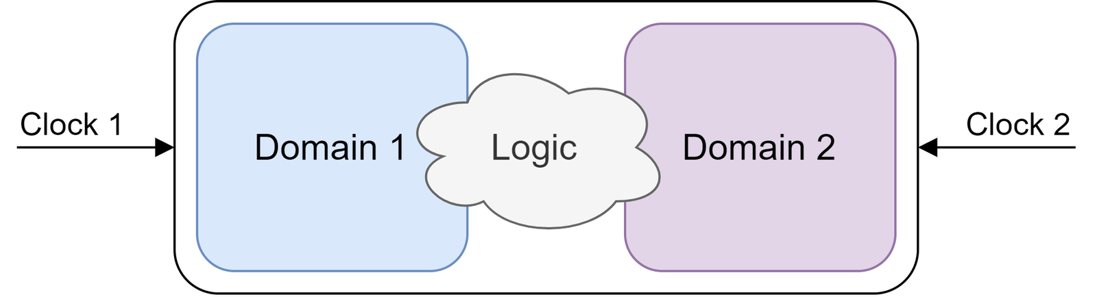
For example, if all flip-flops in a design are clocked by a single global signal, such as the primary clock input of the FPGA, the design operates within a single clock domain. However, if the design receives two separate clock signals—say, one for “Domain 1” and another for “Domain 2″—then it encompasses two distinct clock domains as illustrated in Figure 1.
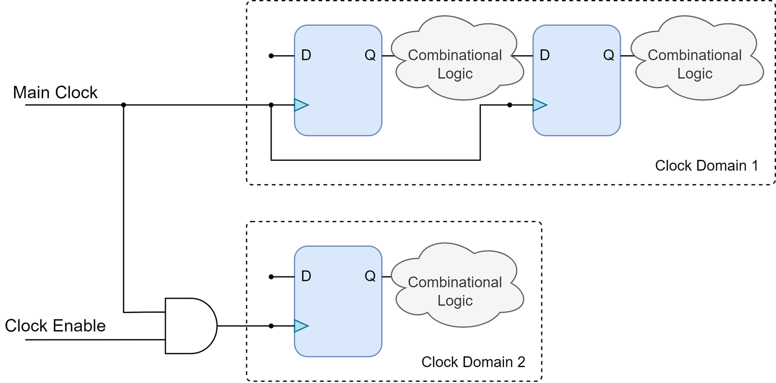
Additionally, constructs like gated clocks, derived clocks, and event-triggered flip-flops are all considered separate clock domains. As illustrated in Figure 2, a simple gated clock can create a new clock domain. While this approach is generally discouraged in FPGA design—where clock-enable signals are preferred for controlling flip-flop activation—it effectively demonstrates the principle of forming separate clock domains.
Clock Domain Crossing Issues
The first and most critical challenge in managing multiple clock domains is ensuring safe and reliable signal transfer between them. Clock domain crossing (CDC) can introduce a range of complex issues, making it a significant concern in digital design. Several factors contribute to the difficulty of CDC:
- Unpredictable Failures: In systems where clock domains are asynchronous, failures tend to be non-deterministic and difficult to reproduce. These issues typically arise due to the unpredictable alignment of clock edges between domains. Since the clock sources often originate externally and are unrelated to the FPGA’s internal logic, synchronization becomes more complex.
- Technology-Dependent Behavior: The likelihood and nature of CDC-related issues can vary depending on the target technology. For instance, higher-speed technologies—featuring tighter setup and hold timing—may statistically experience fewer metastability issues compared to slower ones. However, this is not guaranteed, as other implementation-specific factors, such as output buffering schemes of synchronous elements, can also significantly influence failure rates.
- Limitations of EDA Tools: Electronic Design Automation (EDA) tools generally do not automatically detect CDC problems. Static timing analysis tools primarily focus on timing within individual clock domains, and interclock timing checks must be explicitly defined by the designer. Without proper configuration, CDC issues may go unnoticed during the design flow.
- Debugging Complexity: Cross-domain failures are inherently challenging to identify and diagnose, especially if the designer is unfamiliar with the underlying mechanisms. Therefore, it is essential to clearly define and implement all inter-domain communication strategies before synthesis and place-and-route phases begin.
Before diving into solutions, it’s important to understand what can go wrong when transferring signals between clock domains. Consider the example illustrated in Figure 3, where a signal is passed from one clock domain to another.
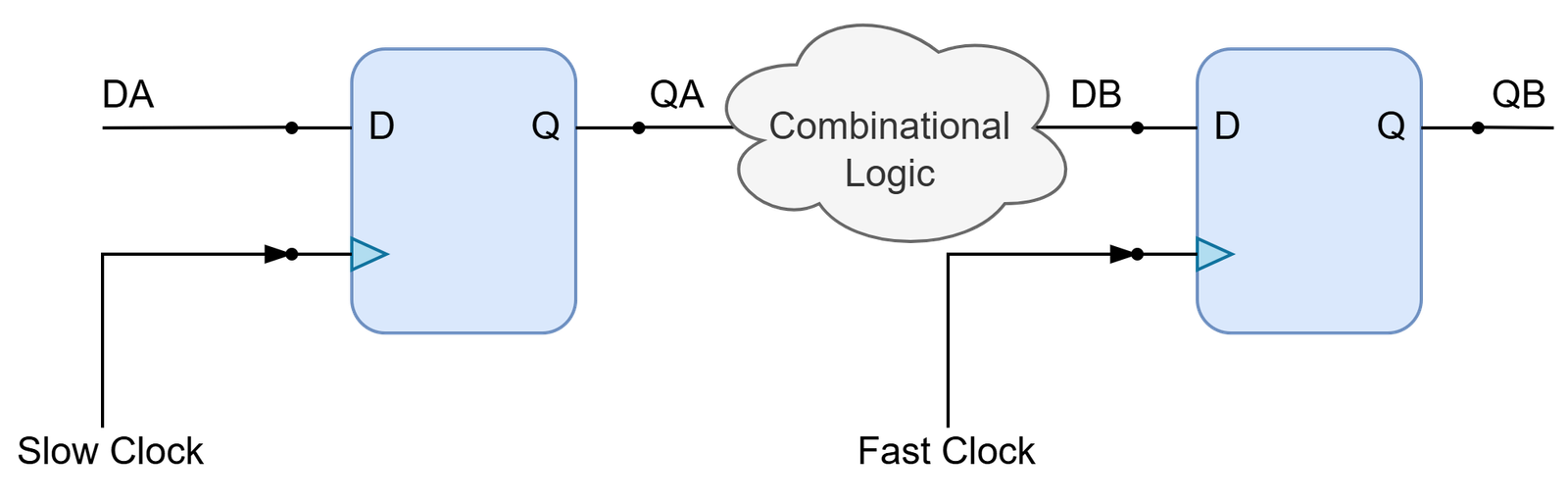
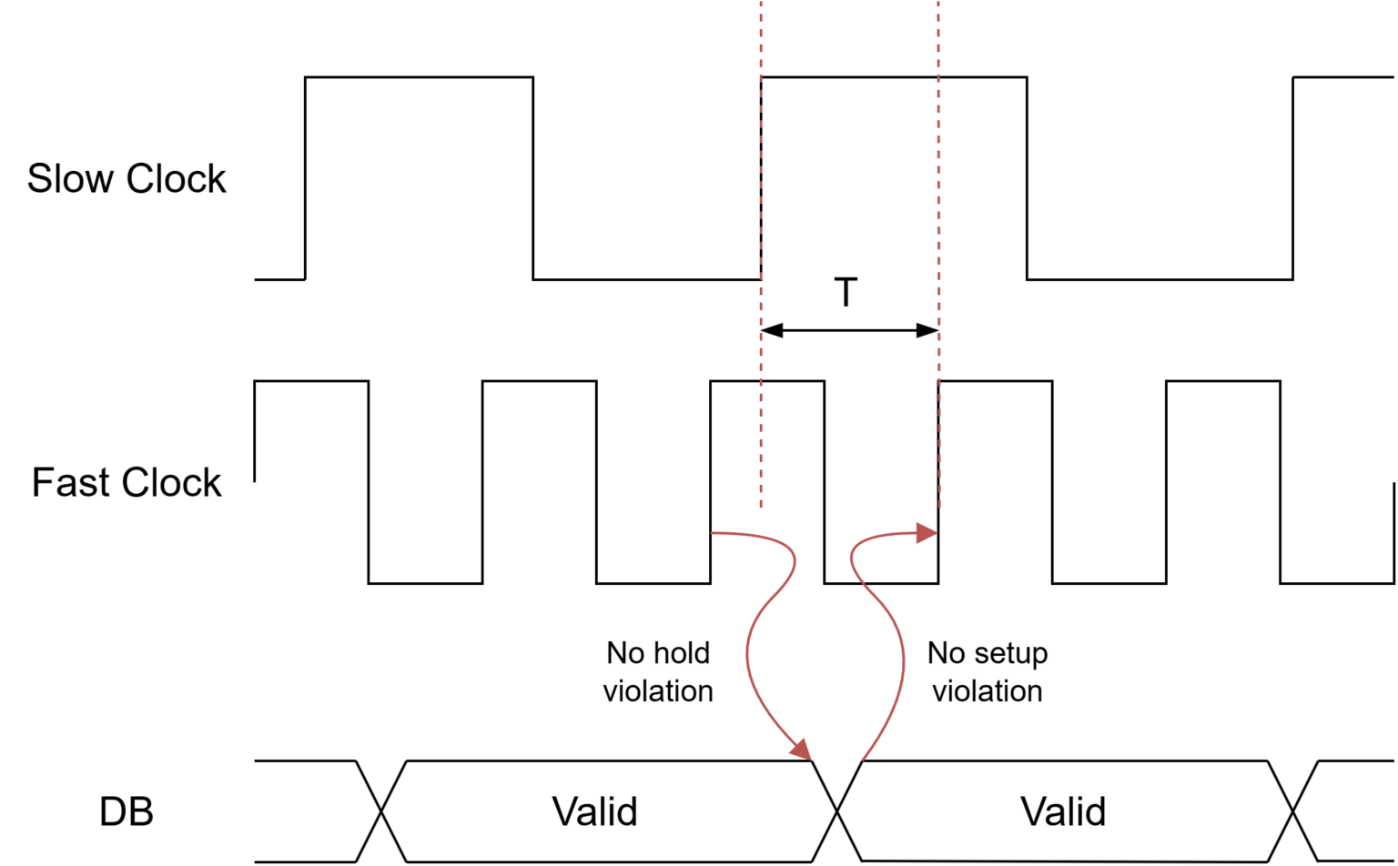
Figure 4 depicts a situation where the slow clock has exactly twice the period of the fast clock. In this configuration, the time between the rising edge of the slow clock and the rising edge of the fast clock—denoted as T—remains constant, assuming no frequency drift occurs. Because the clocks are phase-aligned, T stays fixed and, in this case, is greater than the combined logic delay and the setup time of the flip-flop driven by the fast clock. As a result, signal transitions occur safely without violating setup or hold timing constraints.
However, this stable behavior depends entirely on the initial phase relationship established when the clocks power up. If, upon startup, the phase alignment differs—as shown in Figure 5—then the timing between clock edges can shift unfavorably, potentially leading to violations. This misalignment can cause the rising edge of the fast clock to sample the signal during an unstable period, resulting in metastability or data corruption.
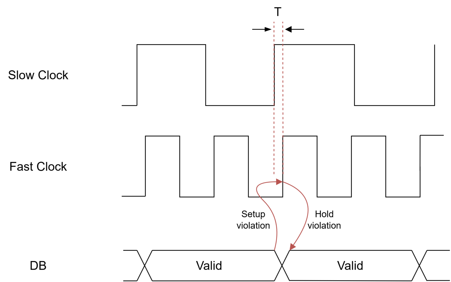
Such scenarios are not limited to clocks with integer frequency relationships; they can occur between any two clock domains, regardless of frequency. The key difference is that, with mismatched frequencies, these timing violations tend to occur less predictably and do not follow a regular pattern.
Ultimately, clock synchronization issues are often non-deterministic and difficult to replicate. This unpredictability undermines the reliability of the FPGA design unless proper synchronization techniques are employed from the outset.
What is Metastability?
A timing violation arises when the input data to a flip-flop changes during a critical time window surrounding the active clock edge, as defined by the setup and hold time constraints. When either of these timing requirements is violated, it can cause an internal node within the flip-flop—whether internal or externally accessible—to enter an undefined voltage state.
In such cases, the flip-flop’s transistors may fail to resolve the input into a definitive logic-0 or logic-1 value. Instead of driving the output to a stable high or low level, the internal circuitry may temporarily reside at an intermediate voltage, potentially for an unpredictable duration, before eventually settling to a valid logic level—one that may or may not be correct.
This phenomenon is known as metastability, and it poses a significant threat to the reliability of synchronous systems. An example of such behavior is depicted in Figure 6 where DB is the input and QB is the output of the second flip-flop shown in Figure 3.

As illustrated in the waveform diagrams, when a data transition occurs within the setup and hold violation window, the output of the flip-flop may temporarily rise to an indeterminate voltage level—one that does not represent a valid logic-0 or logic-1. If the flip-flop includes an output buffer, this metastable behavior might manifest as a spurious transition at the output while the internal node attempts to resolve to a stable state.
The duration for which a signal remains metastable is inherently probabilistic. In some cases, the signal may remain in this undefined state for nearly the entire clock cycle. If such a metastable output is propagated into downstream combinational logic, the result can be unpredictable, as logic gates might interpret the ambiguous voltage differently based on their threshold sensitivities.
From a timing analysis perspective, standard assumptions hold that the propagation delay between flip-flops must be less than the minimum clock period. However, metastability introduces additional, unaccounted-for delays, effectively consuming the timing margin of the critical path. This can lead to severe functional failures that are difficult to detect, as their manifestation depends heavily on the relative timing of clock edges between domains.
A critical challenge in FPGA design is that the effects of metastability are not easily captured in simulation. Most digital simulators do not model analog behavior and therefore do not detect setup or hold violations unless explicitly defined. RTL simulations, in particular, assume ideal timing and do not account for metastability at all. Even gate-level simulations that do flag timing violations may struggle to replicate the specific asynchronous conditions required to trigger a synchronization fault—especially if the engineer is not actively looking for such issues.
This highlights the importance of designing with robustness and reliability in mind. Rather than relying solely on simulation to catch synchronization problems, designers must proactively implement proven CDC strategies. The remainder of this chapter explores various techniques to mitigate metastability and ensure safe communication across clock domains.
Clock Domain Crossing Techniques
1. Phase Control
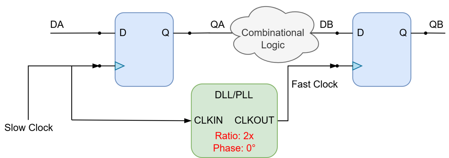
When working with two clock domains that operate at different frequencies and possess an arbitrary phase relationship, the risk of timing violations becomes significant. However, if at least one of the clocks is generated internally—using a Phase-Locked Loop (PLL) or Delay-Locked Loop (DLL)—and if one clock’s period is an integer multiple of the other (within the tuning resolution of the PLL or DLL), then phase alignment can be employed to mitigate these issues.
Take, for instance, a case where a signal is transferred from a slower clock domain to a faster one, where the fast clock operates at twice the frequency of the slow clock. In the absence of a defined phase relationship, signal transitions can violate setup or hold time constraints, as previously discussed. By leveraging a DLL to derive the fast clock from the slow one, it is possible to align their phases in a controlled manner.
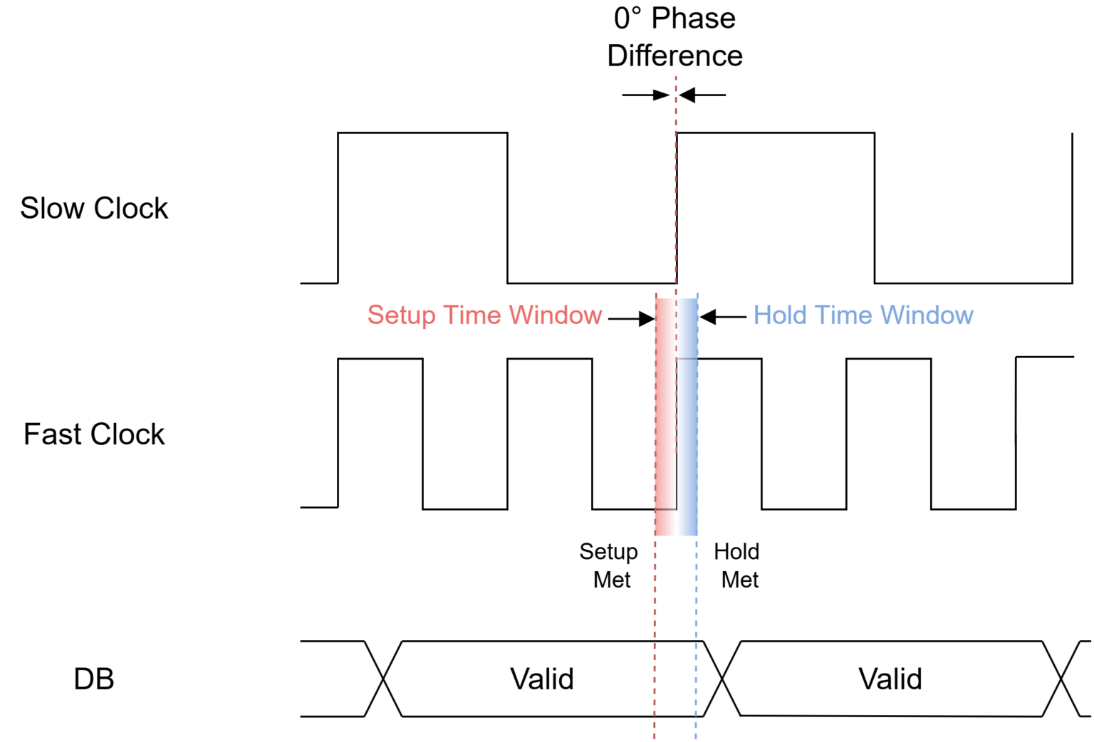
As illustrated in Figure 7, the DLL shifts the phase of the fast (receiving) clock so that it aligns with the slow (transmitting) clock. This phase alignment ensures that the available time window for data transfer, denoted as T, is maximized.
Under these conditions, setup violations are avoided as long as the data propagation delay between the source flip-flop in the slow domain and the destination flip-flop in the fast domain remains less than the fast clock’s period. This is illustrated in Figure 8.
If achieving precise skew control is challenging, especially with regard to hold time constraints, an alternative approach is to capture the incoming signal on the falling edge of the fast clock. This can provide additional margin for setup time, assuming the system still meets the necessary timing requirements.
In many practical scenarios, designers do not have the flexibility to control the phase relationship between clock domains. This limitation is particularly evident when the FPGA operates under strict external timing constraints or when the clock domains have unrelated frequencies. For example, if the FPGA serves as an interface between two systems with tight input and output delay requirements, modifying the phase of either clock may not be feasible. Such situations are quite common in real-world designs, necessitating alternative approaches for managing clock domain crossings. The following sections explore the most widely used techniques for addressing these challenges.
2. Synchronization Chain
In asynchronous clock domain crossings, data arriving from an external or unrelated clock domain may violate setup and hold times of a receiving flip-flop, resulting in metastability. To mitigate this, a chain of flip-flops—commonly referred to as a synchronization chain—is inserted to allow the metastable state to resolve before the signal propagates to downstream logic.
The effectiveness of this synchronization chain is highly dependent on its depth, i.e., the number of cascaded flip-flops. Increasing the number of flip-flops in the chain statistically increases the likelihood that any metastability will decay to a valid logic level before the data is captured by subsequent logic.
Figure 9 illustrates a typical synchronization chain used to safely transfer a single-bit signal between two asynchronous clock domains. On the left, the signal originates from a source domain and is potentially asynchronous with respect to the destination clock. To mitigate the risk of metastability, the signal is passed through a chain of 𝑁 flip-flops (FF_1 to FF_N), all clocked by the destination domain. Each flip-flop stage in the chain provides an additional clock cycle for any potential metastable condition to resolve. The final flip-flop output is then considered stable and safe to be sampled by the destination domain’s combinational logic.

The depth of the synchronization chain, denoted as 𝑁, directly influences the metastability failure probability. Each additional flip-flop stage significantly reduces the probability of metastability propagation, with the reduction being exponential in nature. But each additional flip-flop adds one cycle clock latency to the synchronized signal. In most practical applications, a two-stage synchronization chain provides a sufficient balance between reliability and latency.
3. Asynchronous FIFO
A more advanced technique for transferring data between clock domains involves the use of First-In, First-Out (FIFO) buffers. FIFOs are particularly well-suited for handling multi-bit signal transfers across asynchronous clock boundaries. They are commonly employed in scenarios such as interfacing between standardized bus protocols or performing read and write operations to burst-capable memory systems.
FIFOs are highly versatile data structures, commonly used in a variety of digital systems. However, within the scope of clock domain crossing, their primary value lies in efficiently handling bursts of data that must be transferred between asynchronous clock domains.
A useful analogy for understanding FIFO behavior is the checkout line at a supermarket. Customers arrive at unpredictable intervals, though generally following an average rate. At times, arrivals are sparse, while at others, bursts of customers form. The cashiers, representing the receiving end, cannot immediately serve every customer upon arrival—so a queue forms. In computing terms, such a queue is abstracted as a FIFO. The cashiers proceed at a steady pace, serving one customer at a time, regardless of the queue’s length. If the rate of incoming customers consistently exceeds the rate at which they are served, the line will grow indefinitely unless the system is modified—either by increasing the service rate or reducing the arrival rate.
This same concept applies to data transfers across clock domains. Data may arrive in the transmitting clock domain at irregular intervals, sometimes in large bursts. The receiving side—operating on a different clock—can only process data at its own fixed rate. The FIFO, as shown in Figure 10, serves as the buffer or queue between the two domains.
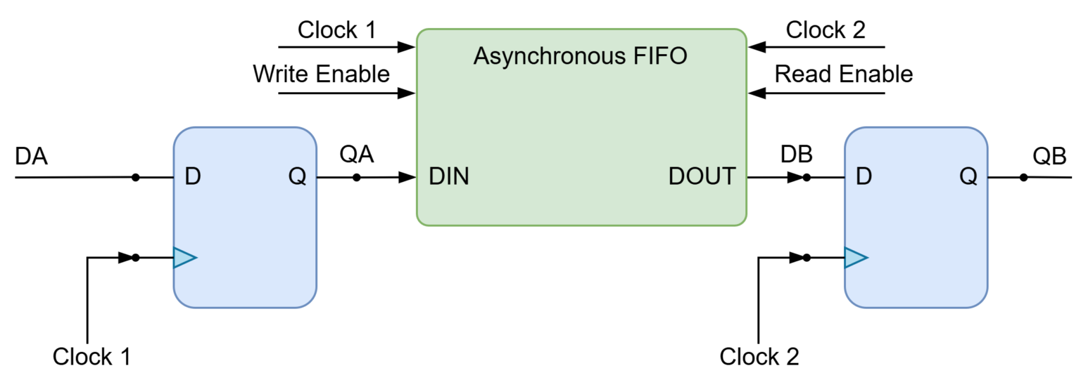
In an asynchronous FIFO configuration, the write (input) and read (output) operations are driven by separate, unrelated clocks. Data is written into the FIFO whenever it becomes available on the transmit side, and it is read out when the receive side is ready to process it. Because the queue has finite storage, overflow must be managed carefully.
There are two primary strategies to avoid FIFO overflow:
- Predefined system parameters: If the burstiness of the incoming data, the minimum consumption rate, and the maximum permissible queue size are known in advance, the FIFO can be sized appropriately to accommodate the traffic.
- Dynamic flow control: Handshaking mechanisms can be used to coordinate data transfer, temporarily halting writes when the FIFO is full or signaling the receiver when data is available to be read.
It is important to understand that an overflow condition can still occur even when the transmitting clock domain operates at a lower frequency than the receiving clock domain. This is because the transmission side may deliver data to the FIFO using fewer clock cycles than the number of cycles required by the receiving side to process that data. Without proper handshaking or flow control mechanisms, such imbalances can lead to FIFO overflow. Therefore, in the absence of dynamic controls, it becomes essential to analyze and account for the worst-case data transfer scenarios to ensure reliable system behavior.
Happy coding.
fpgawizard.com


1 Response
[…] read it: It tackles the hard stuff: Clock Domain Crossing (CDC), timing closure, power consumption optimization, and physical design […]