
DO-254 is the design assurance standard for airborne electronic hardware. Published in 2000 and made mandatory by FAA Advisory Circular AC 20-152 in 2005, it governs the development of any FPGA, ASIC, or complex PLD that ends up on a certified aircraft — from commercial jetliners to military UAVs. If your RTL logic controls a flight surface, a navigation receiver, or an engine FADEC, DO-254 is the process framework your entire program must follow.
The standard defines not what your hardware does, but how you demonstrate it does what it is supposed to do. Every design decision — from module partitioning to simulation coverage — must produce documented evidence that the certifying authority can audit. This post covers the foundation: what DO-254 actually demands, and why the process is structured the way it is.
1. The Standard and Its Scope
RTCA DO-254 (identical to EUROCAE ED-80) was published in April 2000 and applies to Complex Electronic Hardware (CEH) used in airborne systems. The key word is “complex”: DO-254 defines complex hardware as any device for which exhaustive testing of all input combinations is impractical. In practice, any modern FPGA qualifies. A Xilinx Artix-7 with 100,000 LUTs cannot be exhaustively tested; there are more possible input states than atoms in the observable universe.
DO-254 does not apply to simple hardware — discrete logic gates, resistor networks, crystals, passive filters. The boundary matters: a designer sometimes gets to argue that a small PLD performing purely combinational glue logic qualifies as “simple.” That argument requires its own analysis and DER approval. When in doubt, assume DO-254 applies.
The standard applies to the function, not the chip. If a single Xilinx Zynq SoC implements both a flight-critical autopilot function (DAL-A) and a non-critical telemetry logger (DAL-D), the entire FPGA logic must be treated as DO-254 hardware — unless formal partitioning isolates the functions completely. Partitioning is hard to prove; most programs avoid it by putting safety-critical logic in dedicated devices.
2. The V-Model Lifecycle
DO-254 mandates a V-model development process. The left arm of the V is decomposition and design: System Requirements flow down to Hardware Requirements, then to Conceptual Design, then to Detailed Design, and finally to Implementation (the FPGA bitstream). The right arm is verification: each left-arm artifact has a corresponding review, analysis, or test activity on the right that validates it.
The most important implication of the V-model is that design and verification are planned in parallel, not sequentially. The Hardware Verification Plan is written before the detailed design begins. Test cases are derived from requirements before the RTL is complete. This feels wasteful until you realize why it exists: if you write tests after the design, you are unconsciously testing what the design does rather than what the requirements say it should do. The V-model forces the distinction.
The V also enforces completeness. Every element on the left arm must have a corresponding verification activity on the right. If a hardware requirement has no test case, that is a gap. If a design element has no requirement pointing to it, that is orphan logic — and orphan logic in a safety-critical device is a finding.
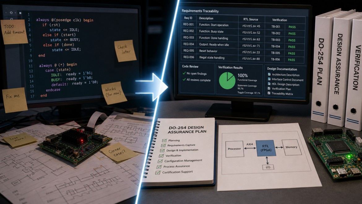
3. Requirements Traceability
Every hardware requirement must trace to the design elements that implement it, and every design element must trace back to a requirement that justifies its existence. This bidirectional traceability is maintained in a trace matrix — a document (or tool-generated artifact) that links requirement IDs to specific modules, signals, and test cases.
In RTL practice, traceability typically means annotating HDL source with requirement IDs. The convention varies by program, but the principle is constant: a reviewer reading the code should be able to answer “which requirement does this signal implement?” and a reviewer reading the requirements should be able to answer “which lines of HDL cover this requirement?”
4. The Evidence Artifacts
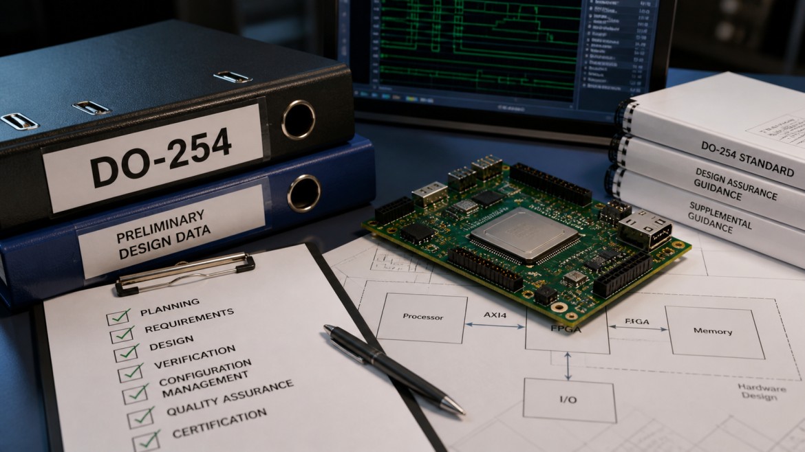
DO-254 defines a specific set of plans and data items that must be produced. Plans are written before design begins and reviewed by the certifying authority before work starts — they establish the rules the program will follow. Data items are produced during and after development and demonstrate that those rules were followed.
The four required plans are: the Hardware Development Plan (HDP, describes how the design will be done), the Hardware Verification Plan (HVP, describes how verification will be conducted), the Hardware Configuration Management Plan (HCMP, describes how artifacts are controlled and changed), and the Hardware Quality Assurance Plan (HQAP, describes how compliance with all plans will be audited). For DAL-A programs, these documents can each run to dozens of pages and require DER review before design begins.
Design data includes the hardware requirements document, conceptual design description, detailed design (HDL source, synthesis netlists, pin assignments), and test vectors. Verification records include simulation reports, structural coverage reports, hardware test reports, and review checklists. Every deviation from expected behavior generates a Problem Report. The program closes with an Accomplishment Summary (HAS) that lists every artifact produced and certifies compliance — this is the document submitted to the DER for final approval.
5. Verification Independence
For DAL-A and DAL-B hardware, the person or organization that performs verification cannot be the same person who performed the design. This is verification independence — and it is organizational, not just individual. On a small team, assigning review tasks to a colleague does not satisfy DAL-A independence; the verifier must be from a separate organization or team with no design responsibility for the artifact being reviewed.
Independence applies to review activities and test execution, not to tool operation. The designer can run the synthesis tool; the independent reviewer must review the synthesis results. The designer can build the simulation testbench; the independent reviewer must review the test cases and the coverage report, not just sign off on the pass/fail result.
For DAL-C, DAL-D, and DAL-E, no independence is required. The same engineer who designed the hardware can verify it. This is one of the practical reasons why DAL-C programs cost significantly less than DAL-A: independence roughly doubles the labor required for every verification activity.
Final Thoughts: Process Is the Product
DO-254 is a process standard, not a technology standard. It does not tell you what gates to use, how to write RTL, or which FPGA family to choose. It tells you what to demonstrate and how to document it. The hardware itself is still your engineering problem — the timing closure, power budget, and functional correctness are all on you.
What DO-254 adds is a framework for proving that your engineering decisions were correct. Every design choice must trace to a requirement. Every requirement must be verified. Every verification result must be independent (at DAL-A/B). And all of it must survive an audit by a certifier who has seen every shortcut in the book. The process looks bureaucratic because it is — and it is because hardware failures in airborne systems have killed people. The paperwork exists so that it does not happen again.
Happy coding.
fpgawizard.com